
products categories

contact us
- If you have questions, please contact us, all questions will be answered
- Tel : 18030236818
- Fax : +86-592 5237901
- Email : dexing@china-dexing.com
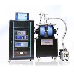
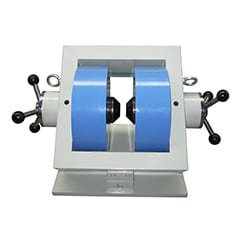
Hall Effect Measurement System
Microwave magnetic field measurement technology on chip surface
Dr. Du Guanxiang is a professor at the School of Communication and Information Engineering, Nanjing University of Posts and Telecommunications. He received his B.S. and Ph.D. degrees from Lanzhou University and the Institute of Physics of the Chinese Academy of Sciences. He is the recipient of the Special Research Fellowship of the Japan Society for the Development of Science. He has worked at Tohoku University in Japan, the University of Basel in Switzerland, and the Max Planck Institute for Biophysical Chemistry in Germany. In 2016, he was employed by the School of Communication and Information Engineering of Nanjing University of Posts and Telecommunications as a Special Professor of the President. He is the first prize winner of Beijing Science and Technology Award, Jiangsu Distinguished Professor, "Dingshan Scholar" of Nanjing University of Posts and Telecommunications, and the 13th batch of "Six Talent Peaks" high-level talents in Jiangsu Province. Currently, he is the deputy director of Jiangsu Peter Grunberg Research Center. Dr Du Guanxiang team committed to the development of practical quantum precision measurement technology, he faces the chip surface magnetic field measurement requirements, proposed the scanning and imaging type two kind of new measuring method, tapered optical fiber is developed sub-micron diamond color NV heart probe and chip surface microwave magnetic field high-resolution high-speed imaging system, realized the high resolution measurement chip surface microwave field, is of great significance to the improvement of chip design and testing ability.

On the other hand, traditional circuit analysis is based on path analysis. In HF devices, the concept of path is challenged by coupling crosstalk and must be shifted to electromagnetic field based analysis. Why do field analysis? First of all, Maxwell's equations do not contain source terms and cannot simulate active devices and nonlinear devices, which makes EDS and other design software unable to truly simulate the real physical environment inside the active components. As far as we know, near field testing is the closest test approach to the real electromagnetic process inside the device that our technology can reach. Moreover, more importantly, the information obtained by software simulation is limited or even completely distorted in high frequency and high complexity devices. This is because the simulation is only a simplification of the real components. As the line width decreases, the skin effect limits the high-frequency current to the edge of the signal line (the skin depth of copper is 670 nm at 10 GHz). Any slight machining defects and the accumulation of the wire along the signal will lead to serious distortion of the simulation results.